
Explore why the memory wall stalls AI progress. Discover how HBM4 16-layer stacking, 2 TB/s bandwidth, and Compute-in-Memory fix modern neural hardware.
Modern bus interfaces like Thunderbolt 5 vs USB4 2.0 push external speeds to 120 Gbps. However, artificial intelligence supercomputers face a much harsher physical barrier. This barrier is known as the memory wall. Frontier large language models now scale into trillions of parameters. Because of this growth, graphics processing units (GPUs) frequently run out of raw data. The real crisis in modern computing is no longer transistor calculation speed. Instead, the bottleneck is how fast data moves between memory chips and compute cores. To solve this issue, engineers are deploying High-Bandwidth Memory (HBM4) and Compute-in-Memory (CIM) architectures.
What Is the Memory Wall in AI Computing?
For over forty years, computers have followed the classical von Neumann model. In this setup, processing cores sit separate from memory pools. Thin copper wires connect the processors to the memory chips on a circuit board. Historically, processor compute speeds grew by roughly 50% every year. In contrast, memory bandwidth only improved by about 7% annually.
This growing gap created the memory wall. High-performance processors can perform hundreds of trillions of calculations per second. Yet, they spend up to 70% of their time idling. They must wait for data packets to cross slow memory buses. Engineers call this issue memory-bound execution.
The Inference Flip and Latency Demands
During the early days of generative AI, companies focused mainly on model training. Training processes large batches of text where raw compute power dominates. Today, the industry has crossed the inference flip. Running live models to answer user queries now takes two-thirds of all AI compute power. Real-time inference is extremely sensitive to delay. Users expect instant answers for voice agents and self-driving cars. As a result, memory speed has become the main commercial bottleneck.
How HBM4 Solves the Bandwidth Bottleneck
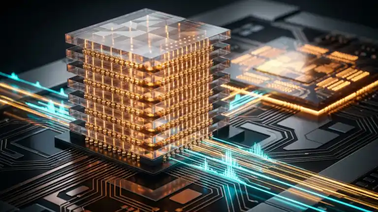
High-Bandwidth Memory (HBM) completely changed traditional memory design. Instead of placing chips flat on a board, HBM stacks DRAM dies vertically. Microscopic conduits called Through-Silicon Vias (TSVs) connect the layers together. These compact vertical stacks sit on a silicon base right next to the GPU core. This shortens data travel distances from inches to millimeters.
The Major Breakthroughs in HBM4
Preceding standards like HBM3e pushed memory speeds to their physical limits. HBM4 introduces three major design upgrades:
- 16-Layer 3D Stacking: HBM4 stacks up to 16 ultra-thin DRAM dies together. This design delivers huge memory capacities of 48 GB to 64 GB per stack.
- 2048-Bit Wide Interface: Older HBM designs used a 1,024-bit memory bus. HBM4 doubles this width to a 2,048-bit bus. This change boosts bandwidth past 2 to 3 Terabytes per second (TB/s) per stack.
- Customized Logic Base Die: Older generations built the base die on standard DRAM processes. HBM4 builds its base die on advanced 3nm and 4nm logic foundry nodes. This upgrade cuts power use and improves signal quality.
Compute-in-Memory (CIM): Processing Without Data Movement
HBM4 widens the data path between memory and the processor. However, it still requires moving billions of bits across physical wires. Moving an 8-bit number across a chip burns 100 times more energy than the math itself. Compute-in-Memory (CIM) solves this problem completely. It performs mathematical calculations directly inside the memory array itself.
Analog Matrix Math in Non-Volatile Memory
Neural networks rely heavily on matrix multiplication. Compute-in-Memory systems use the physical properties of special memory cells to do this math. These cells include Resistive RAM (RRAM) and Magnetoresistive RAM (MRAM):
- Engineers apply voltages across a grid of memory cells. Ohm’s law calculates multiplication instantly in the analog domain.
- Kirchhoff’s current law then adds the currents along each wire in parallel. This design finishes massive matrix math instantly without sending data to an external processor.
Technical Comparison: HBM3e vs HBM4 vs CIM
| Architecture Metric | Standard GDDR6 | HBM3e (Current) | HBM4 (Next-Gen) | Compute-in-Memory |
|---|---|---|---|---|
| Physical Interconnect | Planar PCB Traces | Silicon Interposer TSVs | 2.5D/3D Hybrid Bonding | Internal Crossbar Arrays |
| Interface Bus Width | 32-bit to 64-bit | 1,024-bit | 2,048-bit (Doubled) | Direct On-Die Analog Array |
| Peak Bandwidth (Per Stack) | 50 to 80 GB/s | 1.1 to 1.2 TB/s | 2.0 to 3.2 TB/s | Virtual Unlimited (No Bus) |
| Stack Layer Limit | Planar (Single Die) | 8 to 12 Layers | 12 to 16 Layers | Monolithic 3D Array |
| Base Die Technology | Standard DRAM | DRAM Base Process | 3nm / 4nm Advanced Logic | CMOS Under Memory (CuA) |
| Primary Bottleneck | Bus Congestion | Thermal Density | Packaging Cost & Yields | Analog Conversion Precision |
| Target Deployment | Consumer PCs | Nvidia H100 / B200 | Next-Gen AI Clusters | Ultra-Low-Power Edge AI |
Hidden Engineering Realities in AI Memory
Most tech news covers memory upgrades as simple numbers on a sheet. However, semiconductor factories face three harsh physical limits:
1. Extreme Heat Inside 3D Silicon
Stacking 16 layers of silicon traps intense heat inside the chip. The inner layers of an HBM4 cube have no direct airflow. To stop memory cells from failing, chipmakers now use direct copper-to-copper hybrid bonding. This method removes solder gaps completely to speed up heat dissipation.
2. Packaging Yield Risks
Advanced packaging systems bond eight HBM4 stacks around a single processor. If even one DRAM layer has a flaw, workers must discard the entire expensive processor. Because of this risk, chipmakers build smart self-repair circuits directly inside the base die.
3. Analog Conversion Costs in CIM
Compute-in-Memory performs fast analog math. However, modern AI software still requires digital numbers. Converting analog signals back to digital bits requires large converter circuits (ADCs). In early chips, these converters took up 80% of the die area. Shrinking these converters remains a major engineering challenge.
FAQs
Why can’t GPUs just use more regular DDR5 RAM?
Adding DDR5 RAM adds capacity, but it does not add enough bandwidth. Large AI models need to read trillions of values every second. Standard DDR5 memory tops out near 60 GB/s. In contrast, HBM delivers over 1,000 GB/s per stack to ensure real-time answers.
When will HBM4 memory enter mass production?
Leading manufacturers like SK Hynix, Samsung, and Micron will sample HBM4 chips in late 2025. Mass production and deployment into major AI accelerator systems will ramp up across 2026.
Will Compute-in-Memory replace GPUs completely?
No. Compute-in-Memory will mostly power low-energy edge devices like smart cameras and drones. Massive data centers will still rely on GPUs and HBM for large model training.
Why is liquid cooling necessary for AI memory?
Packing memory stacks tightly next to processors produces immense heat. A single processor socket can generate over 1,000 watts. Standard air fans cannot cool this dense heat fast enough. Therefore, data centers must switch to direct liquid cooling systems.
Key Takings
- The Memory Bottleneck: AI performance is limited by memory transfer speeds rather than raw compute calculations.
- HBM4 Bus Expansion: Doubling the bus width to 2,048 bits pushes memory bandwidth past 2 to 3 TB/s per stack.
- Advanced Logic Base: Moving the base die to 3nm and 4nm nodes merges memory packaging with logic foundry tech.
- Zero-Movement Math: Compute-in-Memory cuts energy costs by performing analog calculations directly inside memory arrays.
- Cooling Demands: Extreme heat density makes hybrid bonding and liquid cooling mandatory for next-generation AI hardware.
Additional Resource
- IEEE Computer Society Microprocessor Architecture Guidelines: Technical reports detailing through-silicon via thermals, 3D packaging standards, and processing-in-memory benchmarks.

Abdulrehman Khalid ✓ Verified Author
Founder & Lead Hardware Analyst at TechWorthies
Abdulrehman Khalid is a technology analyst, hardware researcher, and founder of TechWorthies. With extensive hands-on experience in benchmarking computer hardware, display interfaces, and wireless communications, he specializes in high-speed bus architectures, consumer electronics diagnostics, and emerging AI robotics. His technical guides prioritize empirical lab testing, official standards verification (IEEE, VESA, JEDEC), and actionable troubleshooting for hardware enthusiasts.