
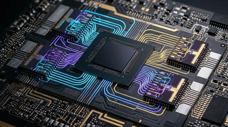
Explore silicon photonics in AI clusters. Learn how optical I/O, co-packaged optics (CPO), and laser waveguides overcome copper interconnect limits.
Artificial intelligence training clusters now connect tens of thousands of accelerators into unified computing fabrics. These massive supercomputers handle generative foundation models and physical AI and robotics. However, as compute performance multiplies, hardware architects face a severe physical bottleneck. GPUs process calculations faster than copper cables can transfer data. This communication choke point compounds the memory wall in AI hardware. To break this electrical barrier, the semiconductor industry is turning to light. Silicon photonics and optical I/O are transforming server architecture. Here is an in-depth breakdown of Silicon Photonics in AI Clusters.
The Physical Copper Barrier in Modern AI Clusters
For decades, data centers used copper traces and Direct Attach Copper (DAC) cables to link compute nodes. Copper has delivered cheap and dependable electrical transmission. However, as speeds reach 800 Gbps and 1.6 Tbps per connection, copper hits fundamental physical limits.
High-frequency electrical signals suffer from severe resistive loss and skin effect. At high transmission rates, electrons travel only along the outer perimeter of copper wires. This resistance turns electrical energy into intense waste heat. Over standard copper traces, an 800G signal degrades completely within one meter. Server designers are forced to install power-hungry retimers and thick cabling to maintain signal clarity.
What Is Silicon Photonics and Optical I/O?
Silicon photonics transfers data using photons of light instead of electrical currents. Engineers fabricate microscopic optical components directly onto standard silicon wafers. This process leverages mature semiconductor manufacturing plants used for computer microprocessors.
An optical I/O link converts electronic data into laser pulses inside microscopic silicon waveguides. The system uses high-speed micro-ring resonators or Mach-Zehnder modulators to encode data onto distinct wavelengths of light. At the receiving end, integrated Germanium photodetectors convert photons back into electrical binary signals. Photons travel across optical fibers with virtually zero electromagnetic interference and minimal heat dissipation.
Co-Packaged Optics (CPO) vs Pluggable Optical Transceivers
Data centers have used pluggable optical transceivers on server front panels for years. However, traditional pluggable transceivers introduce major energy inefficiencies in dense AI clusters:
- Electrical signals must travel through inches of lossy circuit board traces to reach front-panel transceivers.
- Pluggable modules consume between 10 and 15 picojoules per bit (pJ/bit) just to drive copper traces.
- At scale, networking transceivers can consume up to 30 percent of total server rack electricity.
The Architectural Shift to Co-Packaged Optics
Co-Packaged Optics (CPO) eliminates long board traces entirely. Packaging engineers mount the optical engine directly onto the same substrate as the GPU or network switch. Advanced silicon interposers connect the compute die to the optical chiplet across microscopic distances.
This proximity reduces interconnect energy consumption to less than 2 to 5 pJ/bit. Furthermore, optical fibers plug directly into the processor module. This architecture delivers massive bandwidth density while eliminating bulky front-panel transceivers.
Technical Comparison: Electrical Interconnects vs Silicon Photonics
| Interconnect Metric | Passive Copper (DAC) | Pluggable Optical Transceivers | Co-Packaged Silicon Photonics |
|---|---|---|---|
| Physical Medium | Copper Twinax Cable | Fiber via Faceplate Optics | On-Substrate Fiber Waveguides |
| Max Reach at 800G/1.6T | Under 1 Meter | Up to 2 Kilometers | Tens to Hundreds of Meters |
| Energy per Bit | High (Requires Retimers) | 10 to 15 pJ/bit | Under 2 to 5 pJ/bit (Ultra Efficient) |
| Thermal Footprint | Severe Board Heat | High Faceplate Heat | Drastically Reduced Cluster Heat |
| Latency Profile | Low (Short Distance) | Moderate (DSP Overhead) | Ultra Low (Direct Optical I/O) |
| Signal Density | Restricted by Cable Thickness | Limited by Faceplate Slots | Massive Edge Shoreline Bandwidth |
| Ideal Use Case | Intra-rack GPU to Switch | Long-haul Inter-rack Links | Scale-Out AI Supercomputing Fabrics |
What Other Guides Miss: The Hidden Real-World Photonics Hurdles
While the benefits of silicon photonics are clear, commercial enterprise deployment introduces three difficult engineering challenges:
1. Laser Thermal Sensitivity and External Laser Sources
Silicon is an indirect bandgap semiconductor. Therefore, it cannot emit laser light on its own. Engineers must use Indium Phosphide (InP) or Gallium Arsenide laser diodes. However, laser diodes lose efficiency and degrade rapidly at high temperatures. AI GPUs routinely operate at 85 to 100 degrees Celsius under load.
To prevent laser failure, hardware makers use External Laser Sources (ELS). The laser sits in a cool, field-replaceable module on the server faceplate. Optical fibers route cool continuous light into the hot GPU substrate, shielding the laser from thermal stress.
2. Sub-Micron Fiber Alignment and Dust Contamination
Coupling optical fibers to microscopic silicon waveguides requires sub-micron placement accuracy. A microscopic misalignment causes severe optical insertion loss. Furthermore, a single speck of dust can completely block an optical core in data center server rooms. Specialized automated packaging and optical connectors are essential to maintain clean connections.
3. Field Serviceability Constraints
If a traditional pluggable transceiver fails, a technician simply unplugs it and inserts a replacement. In contrast, a failed optical chiplet inside a co-packaged module could render an entire hundred-thousand-dollar GPU board useless. Solving packaging yields and modular serviceability is the final hurdle before mass enterprise adoption.
FAQs
Will silicon photonics replace copper cables entirely?
No. Passive copper remains the cheapest solution for very short links within a single server chassis. However, for connections extending across server racks or clusters, silicon photonics will replace copper entirely. The crossover point is happening at 800 Gbps and 1.6 Tbps speeds.
What is the difference between optical I/O and standard fiber optics?
Standard fiber optics connect separate network switches across long distances. In contrast, optical I/O brings optical technology directly into the compute package. It replaces electrical copper pins on GPU and CPU processors with light beams.
How does silicon photonics impact AI model training times?
Distributed AI training requires constant parameter synchronization across thousands of GPUs. Traditional network latency and packet buffering leave GPUs sitting idle. Silicon photonics provides uniform, low-latency data pipes. This keeps compute units fully utilized, cutting model training times noticeably.
Why can’t silicon emit laser light directly?
Silicon features an indirect bandgap crystal lattice. When electrons drop between energy states, they release energy as mechanical vibrations (phonons) rather than photons of light. Consequently, optical systems must combine silicon with direct bandgap materials like Indium Phosphide to create lasers.
Key Takings
- The Copper Limit: Electrical traces suffer extreme attenuation and heat loss at 800G and 1.6T speeds.
- Photon Efficiency: Silicon photonics transfers data with laser pulses, cutting interconnect power to under 5 pJ/bit.
- Co-Packaged Optics: Mounting optical chiplets adjacent to compute silicon removes lossy board traces and bulky front modules.
- Thermal Architecture: External Laser Sources protect heat-sensitive laser diodes from high GPU operating temperatures.
- AI Cluster Scaling: Optical I/O enables supercomputing fabrics to scale across thousands of nodes with uniform low latency.
Additional Resource
- Optical Internetworking Forum (OIF) Official Standards: Access industry implementation agreements, co-packaged optics frameworks, and next-generation electrical-optical interface standards.

Abdulrehman Khalid ✓ Verified Author
Founder & Lead Hardware Analyst at TechWorthies
Abdulrehman Khalid is a technology analyst, hardware researcher, and founder of TechWorthies. With extensive hands-on experience in benchmarking computer hardware, display interfaces, and wireless communications, he specializes in high-speed bus architectures, consumer electronics diagnostics, and emerging AI robotics. His technical guides prioritize empirical lab testing, official standards verification (IEEE, VESA, JEDEC), and actionable troubleshooting for hardware enthusiasts.